Changing the course of chip packaging history
BT Laminate

MGC global market share
No.1
Resin PCB surpassing ceramic PCBs in functionality BT resin materials
The key to advances in electronic equipment
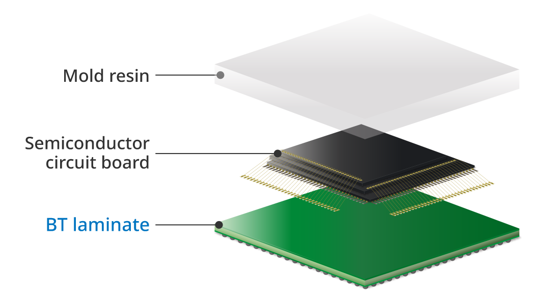
BT laminate sheet has been changed the history of chip packaging.MGC was the first company in Japan to provide resin-based laminate materials for printed circuit boards (PCBs). Laminated materials for PCBs are made of multiple layers of impregnated and dried glass fiber cloth or other base materials that are pressed onto the chip substrate. MGC invented a revolutionary thermal-hardened bismaleimide triazine (BT) resin material that is both low cost and provides excellent thermal and electrical properties. Our BT resin laminate is playing a key role in the advances in electronic equipment and information technology.
01BT resin’s low cost, high thermal resistance, and superior electrical properties raised the standard from ceramic substrates for high-performance semiconductors
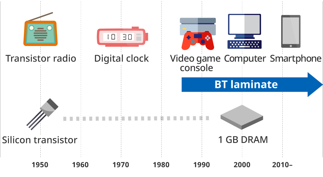
While the world’s elite athletes were vying for medals at the 1976 Montreal Olympics, MGC introduced its revolutionary BT resin that became the gold standard for chip packaging. At the time, the laminated sheet used for the PCBs of high-performance chips was mostly high-cost ceramic. BT resin offered an alternative that exhibited thermal and electrical properties on par with ceramic but at a lower cost. The chip manufacturing industry took notice, and in 1985 BT resin became the first resin laminate material used for chip packaging. Then in the 1990s it rapidly gained acceptance in Japan and worldwide when the industry recognized that in addition to the cost savings, BT resin also simplified the chip fabrication process. BT resin is currently the preeminent laminate material for chip packaging around the world.
02How BT laminate is enabling technological advances for smartphones from the chip up
Any device that has electronic components, from computers and household electronics to automobiles and robots, has one or several built in computer chips. The device makers are constantly seeking to make their products more competitive by making them smaller and lighter while at the same time making them more sophisticated to offer higher performance. You may have a prime example of this in your pocket—smartphone technology evolves with each new model, simultaneously becoming lighter, more versatile, and more powerful.
The makers of the chips inside those devices are constantly seeking ways to advance their chip technology to keep up with manufacturer demand for greater device functionality. Making devices lighter while enhancing performance requires packing more parts into the chip package. This is being made possible by using denser materials that enable decreasing the spacing between the traces on the substrates. Trace spacing has narrowed from over 100 microns to less than 20 microns (1 micron is one thousandth of a millimeter). The biggest challenge when producing PCBs is preventing deformation or curvature caused by temperature change. PCB manufacturing includes processes that alternate hot and cold, and the chip must be made of materials that hold their shape in such conditions. Chips also must be able to maintain their performance specifications without degrading throughout their usage lifetime during the incessant expansion and contraction that occurs each time a device turns on and off. BT resin is a “low warp” material with high structural integrity that performs exceptionally in all aspects. Our BT resin is a key material in the chips that run today’s electronic devices, and we are continuing to develop and advance our BT resin’s capabilities for the technology of tomorrow.
03Aiming for chips with even higher dimension substrate materials for AI and IoT, the future of information technology
Electronic technology is rapidly advancing and information technology is at the very forefront of this revolution.
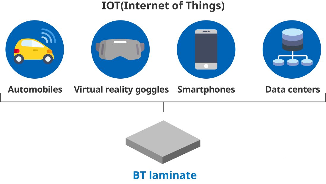
Powerful mobile technology like smartphones are already standard, and wearable devices are just the beginning of the age of the Internet of Things (IoT) and the coming era of artificial intelligence (AI). Each of these technologies represent exponential increases in the volume and complexity of information processing that will require a dramatic revolution in semiconductor technology.
BT laminate is key to the technology breakthroughs that will make these technologies viable. MGC is raising BT resin to a higher dimension. Anticipating the future needs of chipmakers, we are conducting research and development to enhance the functionality of substrates that will provide the foundation for the next leap in information technology.
